Micron Technology has started production of the first memory devices built using IBM’s 3D chip architecture.
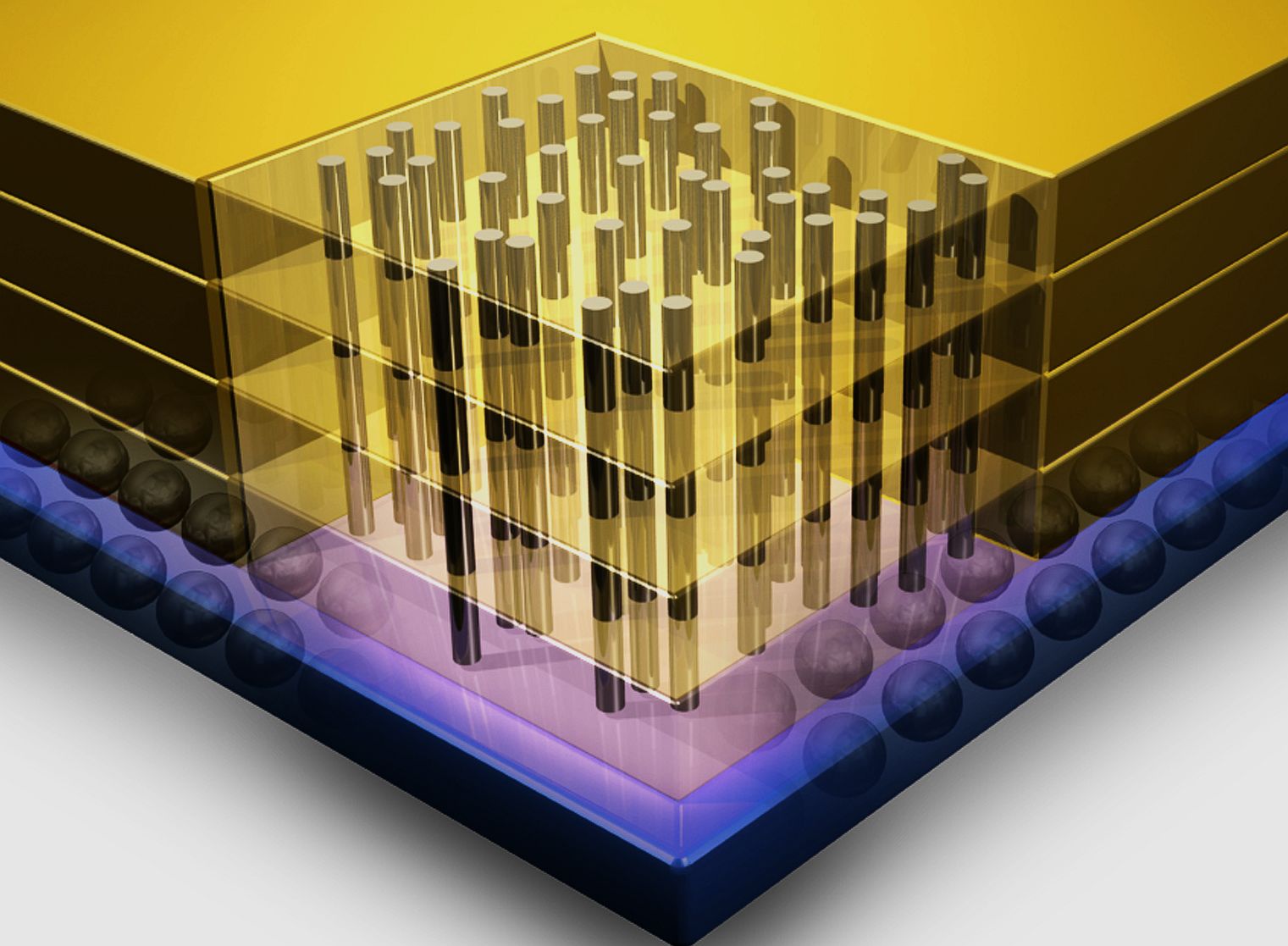
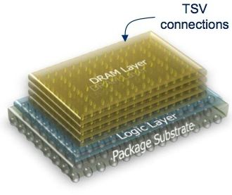
IBM has announced that Micron has started production of its Hybrid Memory Cube (HMC) which uses IBM’s advanced through-silicon vias (TSV), a new chip-making process that creates a 3D micro structure of multiple, stacked layers connected by TSV pipelines – whereas current memory chips are constructed as a single layer.
The 3D architecture effectively stacks several conventional memory chips onto a single mount – increasing density, decreasing volume, and allowing speeds upwards of 15 times faster than normal DDR3 packages.
Advanced TSVs are used as vertical conduits to electrically connect a stack of individual chips. The shortened, on-chip links combined with Micron’s latest DRAM design increases the speed and efficiency of the HMC chip layers when compared to conventional printed circuit board (PCB) connections between separate chips.
According to Micron’s prototype testing results, an HMC chip clocked up a bandwidth of 128 gigabytes per second (GB/s) compared with 12.8 GB/s for a conventional chipset. HMC also consumes 70 percent less energy to transfer data and the footprint of the chip stack is only 10 percent of current PCB-based memory.
Subu Iyer, an IBM fellow, said, “This is a milestone in the industry move to 3D semiconductor manufacturing. The manufacturing process we are rolling out will have applications beyond memory, enabling other industry segments as well. In the next few years, 3D chip technology will make its way into consumer products, and we can expect to see drastic improvements in battery life and functionality of devices.”
HMC parts will be manufactured at IBM’s advanced semiconductor fabrication plant (fab) in East Fishkill, New York State, using the company’s 32nm, high-K metal gate process technology. IBM is due to detail this manufacturing process at the IEEE International Electron Devices Meeting in Washington DC on 5 December.
Robert Feurle, vice president of DRAM Marketing for Micron, predicted, “HMC is a game changer, finally giving architects a flexible memory solution that scales bandwidth while addressing power efficiency. Through collaboration with IBM, Micron will provide the industry’s most capable memory offering.”
After relocating from California to Texas in 2020, Oracle's Larry Ellison now reveals plan to…
Share price hit after Meta admits heavy AI spending plans, after posting strong first quarter…
For third time Google delays phase-out of third-party Chrome cookies after pushback from industry and…
Elon Musk firm touts cheaper EV models, as profits slump over 50 percent in the…
Bad news for Tim Cook, as Counterpoint records 19 percent fall in iPhone sales in…
TikTok pledges to challenge 'unconstitutional' US ban in the courts, after President Joe Biden signs…