Huawei Building Massive Chip R&D Centre In Shanghai

Huawei now developing own chip manufacturing technology as it seeks ways around increasing US restrictions
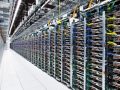
Huawei is building a massive plant in Shanghai dedicated to semiconductor research and development in its latest move to counter increasingly strict chip export restrictions from the US, Nikkei reported.
The site’s activities includes building chip lithography machines, which in the past have been mainly imported into China from companies such as the Netherlands’ ASML and Japan’s Nikon and Canon.
In response to US pressure the Netherlands and Japan have introduced export restrictions intended to cut off the supply of cutting-edge lithography machines to China.
The new R&D centre is located in west Shanghai in a large campus that also houses a major chip development facility and the new headquarters of HiSilicon Technologies, Huawei’s chip design unit, as well as research centres for wireless technologies and smartphones.

Soaring R&D investment
Total investment for the R&D centre alone comes to about 12 billion yuan ($1.66bn, £1.33bn), according to Nikkei, with the overall campus being as big as 224 football fields and having room for 35,000 tech workers, according to the district government.
Huawei is reportedly offering salary packages worth up to twice as much as domestic chipmakers, but one Chinese chip engineer told Nikkei staff would be expected to work “007” hours, meaning midnight to midnight, seven days a week without days off.
“The contract will be for three years, [but] the majority of people can’t survive till renewal,” the engineer said.
Huawei has already hired a number of engineers who have worked with top global chip tool firms including Applied Materials, Lam Research, KLA and ASML as well as chip firms Intel and Micron, Nikkei said.

Engineering talent
Experienced chip talent is increasingly available to Huawei because of restrictions that make it more difficult for Chinese citizens to work for foreign chip companies, the report said.
The R&D site is an indicator of the extent of Huawei’s efforts to counter the effects of sanctions that date back to 2019, when it was placed on the US’ Entity List trade blacklist.
The company initially designed chips and used third-party companies such as Taiwan’s TSMC to manufacture them.
When access to those companies was cut off it turned to domestic chip manufacturer SMIC, which is also under US sanctions, and has now moved a step further by focusing on developing its own chip manufacturing equipment.
Domestic supply chain
The firm’s collaboration with SMIC last year produced a cutting-edge 7 nanometre Kirin chip that powers the Mate 60 flagship smartphone, launched last year to coincide with a visit to China by US Commerce Secretary Gina Raimondo.
That chip is believed to have been produced with older ASML equipment that will eventually become obsolete, making it necessary for companies such as Huawei and SMIC to find new sources of more up-to-date chip manufacturing technology.
Domestic chip firms have begun turning to Chinese tool manufacturing companies such as Naura Technology, and Huawei has invested in other domestic firms as well as carrying out its own chip tech development.