Intel Foundry Assembles Next Gen Chip Machine From ASML

Key milestone sees Intel Foundry assemble ASML’s new “High NA EUV” lithography tool, to begin 14A production
Intel Foundry says it has become the first company to have completed assembly of the first commercial High Numerical Aperture (High NA) Extreme Ultraviolet (EUV) lithography scanner from Dutch giant ASML.
Intel announced that its new TWINSCAN EXE:5000 High NA EUV tool, which is the size of a double decker bus and weighs more than 150 metric tons, is located at its Hillsboro, Oregon, R&D site.
Intel said the massive new machine is now “going through calibration steps in preparation for production of Intel’s future process roadmap.”
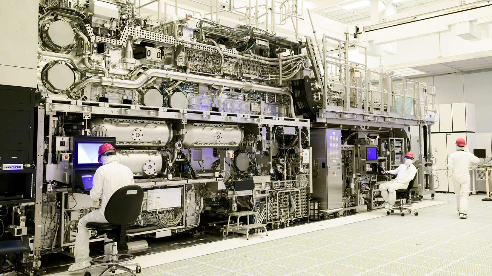
Image credit Intel
TWINSCAN EXE:5000
Intel plans to use the ASML machine in the development of its 14A generation of chips in 2025, with early production expected in 2026 and full commercial production in 2027.
The new tool will give Intel Foundry the ability to dramatically improve resolution and feature scaling for next-generation processors by changing the optics design for projecting printed images onto a silicon wafer.
Essentially the new machine from ASML (which according to Reuters costs 350m euro or $373m) will enable the production of smaller (and hence faster) processors.
“With the addition of High NA EUV, Intel will have the most well-rounded lithography toolbox in the industry, enabling the company to drive future process capabilities beyond Intel 18A into the second half of this decade,” said Mark Phillips, Intel Fellow and director of Lithography, Hardware and Solutions for Intel Foundry Logic Technology Development.

Image credit Intel
Next gen chips
The High NA tools are expected to help shrink chip designs by up to two thirds, and it comes after the recent ASML announcement that it has printed the first-ever 10 nanometer (nm) dense lines in the High NA lab at the company’s headquarters in Veldhoven, Netherlands.
These are the finest lines ever printed, setting a world-record resolution for an EUV lithography scanner, Intel said.
This demonstration validates the innovative High NA EUV optics design from ASML partner Zeiss.
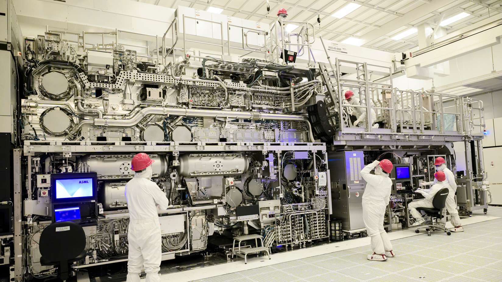
Image credit Intel
It said that groundbreaking images were printed after the tool’s optics, sensors and stages completed coarse calibration – a stepping-stone to running at full specification.
ASML’s ability to print 10nm dense lines with a full field optical lithography system is a key step toward readying the High NA EUV tool for commercial use.
The new machine is expected to be fully up and running later this year after it completes its calibration process.