Ultra Thin Wire Breakthrough Could Lead To Tiny Electronics

Electronic gadgets could get much smaller and thinner thanks to an ultra thin wire developed by researchers
Researchers in the United States have developed ultra thin and flexible metallic wires that are just three atoms wide.
The breakthrough could result in much thinner electronics and smaller processors in the future.
Thin Wires
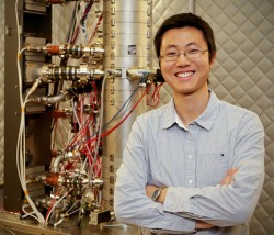
The “smallest wires ever made” were created by a finely focused beam of electrons. The team behind the development was led by Junhao Lin, a Vanderbilt University Ph.D. student and visiting scientist at Oak Ridge National Laboratory (ORNL). The project received most of its funding from a US Department of Energy Office of Science grant.
The flexible metallic wires are only three atoms wide, which is much smaller than what is used in most modern components. For example, it is one thousandth the width of the microscopic wires used to connect the transistors in today’s integrated circuits. Thus this development could herald the arrival of much smaller devices in the future, thanks to tiny components that use electronic circuits made out of atomic monolayers, the thinnest possible form factor for solid objects.
 The thin wire creation was revealed in an article published online on 28 April by the journal Nature Nanotechnology, which detailed how Lin and his colleagues created a new technique to manipulate matter at the nanoscale.
Lin reportedly made the tiny wires from a special family of semiconducting materials that naturally form monolayers. These materials, called transition-metal dichalcogenides (TMDCs), are made by combining the metals molybdenum or tungsten with either sulfur or selenium.
“Junhao took this project and really ran with it,” said advisor Sokrates Pantelides, University Distinguished Professor of Physics and Engineering at Vanderbilt University.
Tiny Circuits
Apparently, atomic monolayers are highly sought after within scientific circles because of their characteristics. This includes exceptional strength and flexibility, transparency and high electron mobility. One of the best-known monolayer materials is graphene, but while graphene is flexible and strong and is considered to be a suitable replacement for silicon, it has so far proven difficult to use it to create electronic circuits.
“This will likely stimulate a huge research interest in monolayer circuit design,” Lin said. “Because this technique uses electron irradiation, it can in principle be applicable to any kind of electron-based instrument, such as electron-beam lithography.”
And it should be remembered that monolayer circuitry is inherently tough and flexible, making this development potentially very important indeed.
That said, it is too early to predict what kinds of applications it will produce, but “If you let your imagination go, you can envision tablets and television displays that are as thin as a sheet of paper that you can roll up and stuff in your pocket or purse,” said Pantelides.
Lin meanwhile thinks that the new technique could make it possible to create three-dimensional circuits by stacking monolayers “like Lego blocks” and using electron beams to fabricate the wires that connect the stacked layers. This video, taken through an electron microscope, shows how narrow ribbons of the monolayer material TMDC form tiny wires only three atoms wide by the process of self-assembly when exposed to a weak beam of electrons.
“Junhao used a scanning transmission electron microscope (STEM) that is capable of focusing a beam of electrons down to a width of half an angstrom (about half the size of an atom) and aims this beam with exquisite precision,” said mentor and ORNL Wigner Fellow Wu Zhou.
How much do you know about microprocessors? Try our quiz.