IBM Shows Graphene Technology In Action
Developments in graphene chips, racetrack memory and transistor size will take us beyond Moore’s Law
IBM has unveiled several working prototypes for chips, memory and transistors that it believes will change the way we compute.
At an IEEE International Electron Devices Meeting this week, scientists from IBM Labs demonstrated the capabilities of three working prototypes, developed in real-world manufacturing environments – a CMOS-compatible graphene device, a sub-10 nanometre (nm) channel length transistor, as well as a Racetrack memory device integrated with CMOS technology on 200mm wafers.
Graphene futures
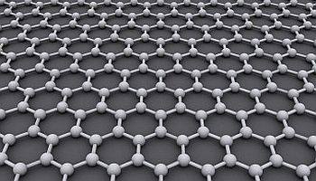
 The graphene integrated circuit demonstrated by researchers is a frequency multiplier and operational up to 5GHz and stable up to 200°C, while the new architecture flips the current graphene transistor structure on its head. “Instead of trying to deposit gate di-electric on an inert graphene surface, the researchers developed a novel embedded gate structure that enables high device yield on a 200mm wafer,” said the company in a statement.
Although detailed thermal stability still needs to be evaluated, IBM believes that “this first-ever CMOS-compatible graphene device can advance wireless communications, and enable new, high frequency devices, which can operate under adverse temperature and radiation conditions in areas such as security and medical applications”.
Carbon Nanotubes
In the demonstration, IBM scientists showed the first transistor with sub-10nm channel lengths, a length scale at which conventional silicon technology has difficulty performing even with new advanced device architectures.
“The scaled carbon nanotube devices below 10nm gate length are a significant breakthrough for future applications in computing technology. While often associated with improving switching speed (on-state), this breakthrough demonstrates for the first time that carbon nanotubes can provide excellent off-state behaviour in extremely scaled devices – better than what some theoretical estimates of tunnelling current suggested,” said the statement.
Racetrack Memory
After seven years of physics research into Racetrack memory, the scientists also demonstrated both read and write functionality on an array of 256 in-plane, magnetised horizontal racetracks.
“This development lays the foundation for further improving Racetrack memory’s density and reliability using perpendicular magnetised racetracks and three-dimensional architectures,” said the company, adding that this breakthrough could lead to a new type of data-centric computing that allows massive amounts of stored information to be accessed in less than a billionth of a second.
Currently, hardware technology is based on the use of silicon circuitry, which according to scientists, is nearing its physical scalability limits. With electronic equipment built on complementary-symmetry metal–oxide–semiconductor (CMOS) technology, IBM believes that new materials and circuit architecture designs compatible with this engineering process are needed if the technology industry is to move forward.
“Today’s breakthroughs,” said T.C. Chen, vice president, Science and Technology, IBM Research in a statement, “Challenge the status quo by exploring the boundaries of science and transforming that knowledge into information technology systems that could advance the power and capability of businesses worldwide.”